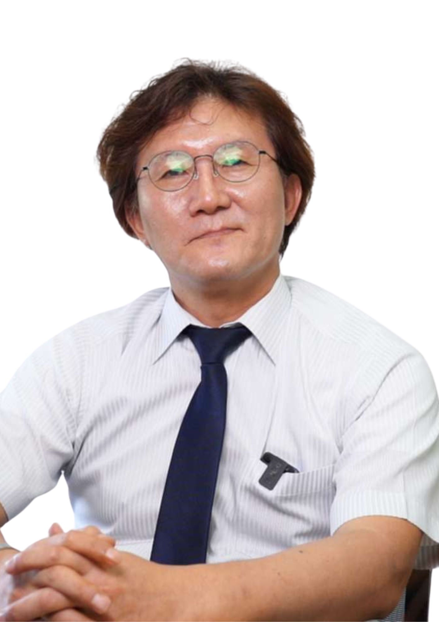
m.hwang@ajou.uz
Education
Hanyang University, 1992
Korea Advanced Institute of Science and Technology (KAIST), 1996
Purdue University, 2007
Work Experience
1995 ~ 2001, Senior Engineer, LG Semiconductor (acquired by SK Hynix), Seoul, Korea
2002 ~ 2002, Supervisor, Korean American Students Association
2003 ~2003, Instructor, Science and Technology for local middle school students, Hillsboro, OR, USA
2004 ~ 2004, Teaching Assistant, Digital Integrated Circuits, Purdue University, IN, USA
2004 ~ 2005, Intern, Qualcomm Inc., San Jose, CA, USA
2005 ~ 2005, Teaching Assistant, Design of Analog CMOS Integrated Circuits, Purdue Univ., IN, USA
2007 ~ 2010, Special Circuit Designer (Team Lead), Intel Corp., Hillsboro, OR, USA
2010 ~ 2016, Principal Engineer (VP), SK Hynix Memory Solutions, CA, USA
2011 ~ 2012, Lecturer on VLSI Circuit Design, Samsung Electronics, Korea
2018 ~ 2022, Freelancer, Multiple locations, CA and OR, USA
2022 ~ Present, Professor, Ajou University in Tashkent
There are many variations of passages of Lorem Ipsum available, but the majority have suffered alteration in some form, by injected humour, or randomised words which.
There are many variations of passages of Lorem Ipsum available, but the majority have suffered alteration in some form, by injected humour, or randomised words which.
There are many variations of passages of Lorem Ipsum available, but the majority have suffered alteration in some form, by injected humour, or randomised words which.